|
|
|
|
OCZ Memory Design and Manufacturing Process Overview |
|
OCZ is the industry leader in designing and producing high speed
memory modules and has been since 2000. We are consistently the first to market with the newest, leading edge products. OCZ memory is specifically
designed for maximum stability in the most demanding of applications. OCZ brand memory products utilize the highest quality
components and the newest design innovations to produce the fastest memory on earth.
|
|
OCZ Memory Module PCB Design
|
|
While most memory manufacturers use standard JEDEC reference
design PCB's, at OCZ the JEDEC reference design is improved
upon. We start by using high quality, 6-layer glass-epoxy substrate PCB, and optimizing the circuit layout. In the case
of our PC2700 REV 2 and PC3000 we use patented ULN (Ultra low noise) shielded PCB.
|
|
OCZ Memory Module Component Selection
|
|
|
At OCZ we work closely with major semiconductor wafer fabrication companies
such as Hynix, Nanya, Micron and Infineon. These companies actually produce the silicon wafer that is contained in the chip
package (the part a customer sees mounted on the PCB referred to as a memory chip). Since they produce the wafer they are able
to provide us with important information about the speed grade of each die and its location on the wafer. This information is
not provided on the outer marking of the chip, and having this information provides us with an edge over our competition.
 
The location of the die on the wafer is important because the dies closer to the center of the wafer typically run much faster
than the chips from the outer part of the wafer. While some companies package their own silicon dies in the casing, label it
with their own markings and speed grade, and place it on the PCB, as seen here
in Kingmax memory, OCZ uses the package provided by the wafer manufacturer because it has proven itself to be the most stable solution available.
After receiving the memory chips at our facility, they are sorted according to their position on the wafer
and then proceed to test the packaged chips to our own internal specifications.
|
|
|
OCZ Memory Module Assembly
|
|
After grading the chips we start our assembly process. Our high quality PCBs are loaded into our automated screen printing machinery
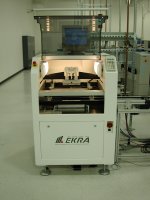
After the screen printing process is completed, the PCB's and memory chips are loaded into our Philips SMT machine, which places the components upon the PCB.
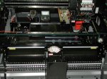
After the finished modules are removed from the SMT ovens they are visual inspected for defects then they are run through our first level of tests.

|
|
OCZ Memory Module testing
|
|
Our first levels of tests are done using our customized
automated CST auto loading test fixture.
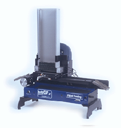
Our first level of testing is done using our customized, automated CST auto loading test fixture. Our first level of module tests qualifies
the memory for DDR 266A (2100), or DDR 333B (2700) operation only. After passing this first level of tests our RAM is sent to our
secondary test and compatibility lab for final testing and speed grading.
|
|
OCZ Memory Module Speed Grading and Motherboard Compatibility Testing
|
|
We speed grade each of our performance series with a combination of Modified CST
Eureka Memory testers and Motherboard based test fixtures. Each module is first tested on our modified memory testers and then run through
a battery of stress tests on motherboard platforms suited to each type of RAM. As new motherboards are released we keep a log of our results
online under our PC2100 & PC2400
and PC2700 & PC3000 motherboard compatibility notes. The motherboard
stress tests that we use to determine maximum stability for our memory that we release to the consumer are as follows:
|
|
- Test 1: Quake 3 Loop
- Test 2: Pass Mark Burn in Test
- Test 3: Sandra Soft Burn in Test
- Test 4: 3DMark2001 From Mad Onion
- Test 5: RC5
|
|
|